
Arm Serial Wire Debug
SWD One data wire, shared in turns
Use SWD to program or inspect an Arm target with a small debug connection. The debugger supplies the clock, while request and response phases take turns on one data wire. A valid wire transaction is only one step: access-port reads can return an earlier result.
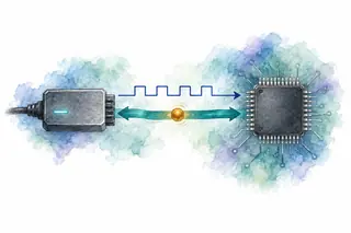
SWD wiring, timing and transaction
Wiring
A debug probe sends SWCLK to the chip debug port. A separate bidirectional SWDIO connection carries request, acknowledgment and data, with only one driver at a time. The probe and target also share ground.
The probe supplies SWCLK, while requests and replies share SWDIO. A turnaround gives the current sender time to release that wire before the other side drives it, avoiding two outputs fighting each other.
SWCLK comes from the probe; neither side drives SWDIO during a turnaround.
SWD ownership
Only one side drives SWDIO. Turnaround transfers ownership.
Read request · 8 clocks. The debugger selects a DP register and the read/write direction.
Timing and model details
46 clocks across shown fields; idle cycles excluded. Field widths are schematic, not proportional to duration. Default one-clock turnaround; ORUNDETECT=0. Read cases select DP RDBUFF; the write selects DP SELECT. WAIT assumes an earlier AP access remains pending; that preceding access sequence is omitted. The target keeps ownership from OK through data and parity during a successful read. SWCLK need not run continuously while idle.
An AP read returns a previous result
Beyond the wire transfer, ADIv5 Access Port reads are posted. Keep the requested address separate from the result returned now.
AP read A→Older value · ignoreAP read B→Value at ADP RDBUFF→Value at BRDBUFF collects the final result without starting another AP access. This separate, simplified sequence assumes the same selected AP, successful accesses, and no intervening SELECT or bank changes. Follow the target’s WAIT and error rules.
When SWD is the smaller connection
JTAG supports scan chains and boundary-scan testing. SWD provides an Arm debug connection with fewer main signal pins.
Check the chip and probe for supported ports. Neither a pin count nor a connector guarantees the target exposes the debug or test feature you need.
Ground is required. Reset, trace, and other optional signals are excluded from these counts.
Explore the JTAG chain →Follow a transaction
Advance here or in the transfer above. The highlighted operation and wire state stay on the same step.
send_request(DP_RDBUFF, READ)
release_for_turnaround()
ack = receive_ack()
if ack == WAIT:
turn_to_host(); return DEFER
word = receive_32_bits()
check_even_parity()
turn_to_host()
return word- Who drives
- Probe drives SWDIO and SWCLK
- Sent so far
- 8-bit DP RDBUFF read request
- Response so far
- ACK not received yet
Debug transfer in progress
Why this step mattersStep 1 of 6, Read request. The request selects a debug-port register and tells the target whether this attempt reads or writes.
Implementation notes
These are probe-level operations, not application CPU loads. Read selects DP RDBUFF after an earlier AP access; write selects DP SELECT. The example uses one-clock turnaround, overrun detection disabled, and valid data parity. WAIT needs bounded retry or deferral. A real driver must also handle FAULT, parity errors, and sticky status using the selected debug-port specification.
Common mistakes
Driving through turnaround
Release SWDIO before the other side takes ownership.
Reading WAIT as zero data
Retry with a bound; WAIT did not return a successful data word.
Ignoring the overrun setting
This lab omits WAIT/FAULT data phases only because ORUNDETECT is disabled.
Trace the driver for every phase, verify request/data parity, then exercise OK and WAIT separately. For a memory read, also track AP selection, posted results, and error recovery.
Further details and primary sources
- Hand off before answering
- The debugger sends the request, then releases SWDIO. After turnaround, the target returns OK, WAIT, or FAULT. On an OK write, another turnaround hands the wire back before the debugger sends data and parity.
- WAIT is not data
- With overrun detection disabled, WAIT has no data phase. Retry with a bound; inspect and clear the documented error state for FAULT. Turnaround defaults to one clock, but debugger and target settings must agree.
- A wire read is not always the requested result
- ADIv5 AP reads are posted: a later AP read returns the previous result, and DP RDBUFF retrieves the final one. Validate even parity and follow the access-port completion rules before interpreting a word as fresh memory data.
Example scope
ADIv5 wire-level examples with one-clock turnaround and ORUNDETECT disabled. Initialization, multidrop selection, power-up, and full error recovery are outside this lab; AP posting is explained but not simulated. SWCLK need not run continuously while idle.
Primary sources
Updated