
Serial Peripheral Interface
SPI Clocked data in both directions
Use SPI for a direct exchange with a selected peripheral, such as a display, converter, or memory. The controller provides the clock while separate data wires carry both directions. Check the peripheral’s clock mode and command framing; adding devices usually adds select pins.
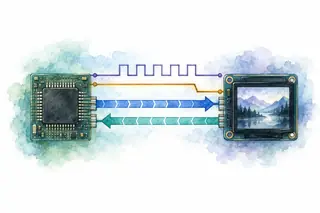
SPI wiring, timing and transaction
Wiring
Four separate signals connect controller and peripheral. SCLK supplies the clock, CS_n selects when low, MOSI sends controller data, and MISO carries the peripheral reply. Ground is a separate connection.
The controller generates SCLK and selects the peripheral with CS_n. Separate MOSI and MISO wires carry outgoing and returning bits during the same clock cycles; the peripheral’s command format determines what those bits mean.
SCLK, chip select and MOSI go to the peripheral; MISO returns data while all devices share ground.
SPI timing
Select a device, exchange eight bits, then release it. Change the mode or skip selection to compare.
Clock configured to mode 0; CS_n is LOW. The first bit must already be valid before the first leading edge.
Timing and model details
Eight-bit, MSB-first fixture. The selected, mode-matched peripheral returns 0x3C while the controller sends 0xA5. The fault deliberately leaves CS_n high and assumes the peripheral releases MISO; external bias may affect the measured voltage, so no received byte is predicted. The two-cycle inset follows the selected bit. In CPHA=1 modes, gray dashes precede the first data launch. Edges are schematic; actual data settles after launch and must meet setup/hold limits.
Four modes, two decisions
CPOL sets idle LOW (0) or HIGH (1). CPHA selects leading-edge sampling (0) or trailing-edge sampling (1). Amber marks the sample edge.
The leading edge leaves idle; the trailing edge returns to idle. Match both settings to the peripheral. Mode 0 needs the first bit valid before the first rising edge.
A shared clock or agreed bit time?
SPI supplies the sampling clock, which suits clocked peripherals such as converters and memories. UART reconstructs timing from a start bit and the agreed baud rate.
Choose the interface the device supports. SPI’s command format and chip-select boundaries still come from its data sheet.
Compare UART framing →Follow a transaction
Advance here or in the transfer above. The highlighted operation and wire state stay on the same step.
rx = []; set_mode(0)
set_cs(LOW)
for bit in msb_first(0xA5):
drive_mosi(bit)
rx.append(sample_miso())
set_cs(HIGH)
return rx- Who drives
- Controller: SCLK/MOSI/CS_n; peripheral: MISO
- Sent so far
- No data clocks yet
- Response so far
- No bits sampled yet
Exchange in progress
Why this step mattersStep 1 of 10, Configure and select. Mode 0 sets idle clock polarity and the sampling edge before CS_n goes LOW.
Implementation notes
The loop expands what an SPI controller does; firmware usually submits a buffer. Mode 0 samples on rising edges. The first bit must already be valid before the first leading edge. A deselected target is modeled as high impedance, not a fixed 0xFF reply. Real pull resistors and device rules determine the line level. Interpret received bytes using the peripheral’s command and status format.
Common mistakes
Matching speed but missing the mode
Both ends must agree on clock polarity and the sampling edge.
Releasing chip select too early
Keep it asserted for the command boundary required by the device.
Expecting an immediate reply
The simultaneous incoming byte may be a prepared value or belong to an earlier command.
Decode both directions using the selected mode. Check the first bit, all eight sample edges, chip-select setup/hold, and MISO release before selecting another device.
Further details and primary sources
- Polarity names the idle level
- Clock polarity, CPOL, sets SCLK idle low or high. The leading edge leaves idle; the trailing edge returns to it. These names still work when a rising edge becomes a falling edge.
- Phase names the sample edge
- Clock phase, CPHA, selects leading-edge sampling when zero and trailing-edge sampling when one. Modes 0/1 idle low; modes 2/3 idle high. Mode 0 needs the first data bit ready before the first rising edge.
- The device defines the message
- Read the peripheral contract for bit order, word length, chip-select timing, command fields, and dummy clocks. SPI itself supplies no universal address or acknowledgment byte. An unselected device must release a shared MISO line as specified.
Example scope
Conventional four-wire, active-low-select SPI; eight-bit, most-significant-first examples. Three-wire, daisy-chain, dual/quad data, and device-specific protocols need their own timing rules. There is no single safe clock rate for every SPI device.
Primary sources
Updated