Shifting the address twice
Check whether the driver expects the 7-bit address or a prepared address byte.

Your next page is on its way.
Firmware / Communication, storage and debug
From I²C sensors to Ethernet networks: explore nine interfaces, their connections, and the transactions firmware sees.
A processor needs to configure sensors, read storage, join a network, and program or test hardware. Each interface defines how to choose a destination, time the bits, and share the connection.
Select an interface to explore its wiring and a step-by-step transfer.
Devices share SCL (clock) and SDA (data). The controller sends an address; the matching device responds on those same wires.
ExampleRead a temperature sensor and a memory on one bus.
Clock and data lines can be shared, but each peripheral usually has its own chip-select line. Separate MOSI and MISO wires carry data in opposite directions.
ExampleSelect a display or serial flash, then exchange data.
One device’s TX connects to the other’s RX. Each end times the bits with its own clock, so both must agree on baud rate and frame format.
ExampleRead boot messages from a microcontroller’s debug console.
Clock and state-control signals reach every chip. Data shifts through a selected register in each chip, then returns to the probe.
ExampleCheck board connections with boundary scan or debug a chip.
The probe supplies SWCLK. The probe and target take turns driving SWDIO; this single data wire carries both requests and replies.
ExampleFlash firmware, set a breakpoint, or inspect a core register.
The host discovers and configures a device, then schedules packets to its endpoints. For USB 2.0, D+ and D− form one data pair—not separate TX and RX wires.
ExampleA computer requests a block of data from a USB device.
Each board has its own cable link to a switch port. Frames use MAC addresses; a switch forwards between ports.
ExampleA measurement board sends readings to a computer on the same network.
Every transceiver taps the same CAN_H/CAN_L pair. Arbitration picks the sender; receivers filter messages by identifier.
ExampleA motor controller and a sensor share one terminated bus.
CMD carries requests and responses. DAT lines carry memory blocks or SDIO bulk data; CMD52 is a one-byte exception carried in the response.
ExampleA logger reads a storage sector; a wireless module exposes SDIO registers and FIFOs.
Signal counts exclude power, ground, and optional pins. MCU = microcontroller; probe = debugger. USB here means USB 2.0 full-speed.
Connecting peripherals? Compare I²C’s shared address bus, SPI’s chip selects, and UART’s link without a clock wire.
Programming or testing chips? JTAG scans a chain; SWD is the compact Arm debug connection.
Inter-Integrated Circuit
Use I²C when several peripherals need to share a few controller pins. An address selects a sensor or memory on the same clock and data pair. This saves select pins, but address compatibility and the electrical load still need checking.
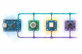
The controller, sensor at address 0x48 and memory at address 0x50 each connect to SCL, SDA and common ground. SCL and SDA each have a separate pull-up resistor to VDD. Every device can pull a line low or release it.
All three devices share SCL for timing and SDA for addresses and data. An open-drain output can pull a line LOW or release it; the pull-up then restores HIGH so another device can safely take its turn.
Dots mark connections; curved crossings keep SCL, SDA and ground electrically separate.
Choose an address. Step through the write and its acknowledgments.
START: SDA falls while SCL stays high.
One controller; ready targets at 0x48 and 0x50; 0x2A accepted as a single data byte. 18 clock pulses in this attempt. START and STOP are line conditions. Address and data windows each show eight bits followed by acknowledgment. For data bits, SDA changes only while SCL is low. Timing is idealized; rise time, setup/hold, arbitration and stretching are not simulated.
The first byte combines a 7-bit address with one direction bit. The acknowledgment comes on a separate clock.
(0x48 << 1) | 0 = 0x907 address bits + 1 direction bitCheck the driver API: some take 0x48 and shift it for you; others expect an address byte. Shifting twice selects the wrong address.
For two conventional peripherals, compare the signals needed at the controller:
I²C saves pins by putting a distinct target address on shared wires. SPI uses a select for each target and can move data in both directions together.
Excludes power and ground. Device support, bus loading, and required throughput still decide the choice.
Compare SPI timing →Advance here or in the transfer above. The highlighted operation and wire state stay on the same step.
start()
send(0x90) // address + W
if not read_ack():
stop(); return NO_TARGET
send(0x2A)
if not read_ack():
stop(); return DATA_NACK
stop()
return OKWrite in progress
Why this step mattersStep 1 of 6, START. START makes every target listen for the next address.
These calls describe controller operations, not a specific driver API. Firmware normally configures a peripheral and checks its status. The teaching targets accept one byte directly; real devices may need command or register bytes. Bound waits for bus availability and completion. DATA_NACK is shown as a defensive branch; the two responding fixtures always accept 0x2A.
Check whether the driver expects the 7-bit address or a prepared address byte.
Check rise time, bus capacitance, and the pin’s low-level current limit.
Check the address, target readiness, and whether a read is intentionally ending.
Capture START, address, receiver ACK, payload, and STOP. Then test a missing target and a bounded wait for stretched SCL. Check analog rise time as well as the decoded bytes.
Conventional open-drain, 7-bit I²C teaching model. Addresses and payload are fixtures, not real device commands. Register formats and recovery procedures belong to each device manual; high-speed and Ultra Fast-mode variations are outside this lab.
Serial Peripheral Interface
Use SPI for a direct exchange with a selected peripheral, such as a display, converter, or memory. The controller provides the clock while separate data wires carry both directions. Check the peripheral’s clock mode and command framing; adding devices usually adds select pins.
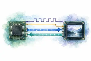
Four separate signals connect controller and peripheral. SCLK supplies the clock, CS_n selects when low, MOSI sends controller data, and MISO carries the peripheral reply. Ground is a separate connection.
The controller generates SCLK and selects the peripheral with CS_n. Separate MOSI and MISO wires carry outgoing and returning bits during the same clock cycles; the peripheral’s command format determines what those bits mean.
SCLK, chip select and MOSI go to the peripheral; MISO returns data while all devices share ground.
Select a device, exchange eight bits, then release it. Change the mode or skip selection to compare.
Clock configured to mode 0; CS_n is LOW. The first bit must already be valid before the first leading edge.
Eight-bit, MSB-first fixture. The selected, mode-matched peripheral returns 0x3C while the controller sends 0xA5. The fault deliberately leaves CS_n high and assumes the peripheral releases MISO; external bias may affect the measured voltage, so no received byte is predicted. The two-cycle inset follows the selected bit. In CPHA=1 modes, gray dashes precede the first data launch. Edges are schematic; actual data settles after launch and must meet setup/hold limits.
CPOL sets idle LOW (0) or HIGH (1). CPHA selects leading-edge sampling (0) or trailing-edge sampling (1). Amber marks the sample edge.
The leading edge leaves idle; the trailing edge returns to idle. Match both settings to the peripheral. Mode 0 needs the first bit valid before the first rising edge.
SPI supplies the sampling clock, which suits clocked peripherals such as converters and memories. UART reconstructs timing from a start bit and the agreed baud rate.
Choose the interface the device supports. SPI’s command format and chip-select boundaries still come from its data sheet.
Compare UART framing →Advance here or in the transfer above. The highlighted operation and wire state stay on the same step.
rx = []; set_mode(0)
set_cs(LOW)
for bit in msb_first(0xA5):
drive_mosi(bit)
rx.append(sample_miso())
set_cs(HIGH)
return rxExchange in progress
Why this step mattersStep 1 of 10, Configure and select. Mode 0 sets idle clock polarity and the sampling edge before CS_n goes LOW.
The loop expands what an SPI controller does; firmware usually submits a buffer. Mode 0 samples on rising edges. The first bit must already be valid before the first leading edge. A deselected target is modeled as high impedance, not a fixed 0xFF reply. Real pull resistors and device rules determine the line level. Interpret received bytes using the peripheral’s command and status format.
Both ends must agree on clock polarity and the sampling edge.
Keep it asserted for the command boundary required by the device.
The simultaneous incoming byte may be a prepared value or belong to an earlier command.
Decode both directions using the selected mode. Check the first bit, all eight sample edges, chip-select setup/hold, and MISO release before selecting another device.
Conventional four-wire, active-low-select SPI; eight-bit, most-significant-first examples. Three-wire, daisy-chain, dual/quad data, and device-specific protocols need their own timing rules. There is no single safe clock rate for every SPI device.
Universal Asynchronous Receiver/Transmitter
Use UART when two devices need a simple byte stream without a clock wire, such as a console or module command link. Start and stop bits give each receiver a timing reference. Both ends must agree on framing and baud rate, and software must define complete messages.
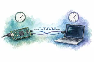
Device A TX connects to Device B RX. Device B TX connects to Device A RX. The devices share ground but each uses its own clock; there is no clock wire.
Connect each TX output to the other device’s RX input. With no shared clock wire, both ends must agree on the baud rate and frame format; each receiver uses its own clock to sample incoming bits.
Match the baud rate and connect compatible logic-level pins; RS-232 and RS-485 require transceivers.
8N1: one start bit, eight data bits, one stop bit. Data travels b0 first.
Start = 0. The falling start edge establishes the receiver’s sampling schedule.
Logic-level UART; 8 data bits, no parity, 1 stop bit. Bit time = 1 / baud; frame time = 10 / baud. Amber markers are ideal sample centers, not a specific receiver oversampling implementation. A high stop bit does not prove the payload is correct. Payload ceiling assumes back-to-back frames with no flow-control pauses. Narrow screens split the same continuous frame into consecutive windows.
A UART frame spends time on framing as well as payload. This worked example uses 8N1 at 115,200 baud.
115,200 ÷ 10 = 11,520 B/sMaximum one-direction payload with continuous framesOne frame takes about 86.8 µs. Idle gaps and application headers reduce useful throughput; baud is not bytes per second.
The active bridge buffers and translates between USB packets and UART bytes. A USB connector and logic-level TX/RX are different electrical and protocol interfaces.
UART is useful for logs and module commands. Software must add any message boundaries, checksums, or acknowledgments it needs.
Compare USB transactions →Advance here or in the transfer above. The highlighted operation and wire state stay on the same step.
value = 0; wait_for_start_low()
for b in 0..7:
value[b] = sample_center()
if sample_stop() != HIGH:
return FRAMING_ERROR
return received_byte(value)Receiving data
Why this step mattersStep 1 of 10, Detect START. The falling start edge gives the receiver a reference for its own sampling clock.
This is a conceptual hardware receiver, not a software timing loop. Firmware configures baud rate and 8N1, then reads received data with its framing and overrun status. The bad-stop fixture forces the final sample LOW; it does not simulate a particular baud mismatch. Define a policy to discard, flag, and resynchronize after errors. UART framing provides no acknowledgment or end-to-end checksum.
Each transmitter connects to the other device’s receiver.
Use a suitable transceiver; the electrical signals differ. RS-485 also needs its own transceiver.
A correctly framed 8N1 byte can still contain wrong data.
Measure a bit interval, decode the known byte, and inspect the stop sample. Exercise back-to-back traffic and receive-buffer overrun; include clock tolerance and interrupt-service latency in the design.
Logic-level, non-inverted 8N1 UART. The selectable rates are teaching inputs, not guaranteed operating points. Voltage compatibility, oversampling, error tolerance, and optional RTS/CTS hardware flow control are target-specific.
Joint Test Action Group · IEEE 1149.1
Use JTAG to inspect a chain of devices or test board connections that are difficult to probe. Shared clock and control signals move data through each device’s selected register. The instruction determines what is scanned, so chain order and register lengths are part of the setup.
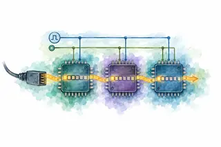
The debugger has separate TCK and TMS outputs, each connected in parallel to Device A and Device B. Curved crossings are not junctions. Data out enters A TDI, passes through A selected register and TDO, then B TDI, selected register and TDO, and returns to debugger data in.
The blue TCK and TMS branches deliver the same clock and state-control signal to both chips. The amber serial chain instead passes through each chip’s selected register before returning to the debugger.
TCK and TMS go to both chips; selected registers form the serial chain, with common ground and optional reset omitted.
Capture, shift six bits through the chain, then update the output latches.
Captured A=101 and B=011. Output latches remain unchanged.
Two fictional three-bit data registers; captured cells 101011; serial input 110100. Cells are drawn from TDI on the left to TDO on the right. Capture and shift leave separate output latches unchanged. Intermediate TAP states and instruction loading are omitted, so the conceptual Capture and Update buttons do not represent single-clock transitions. Not every JTAG data register drives physical pins.
Count the register selected inside each chip. Changing an instruction can shorten the path without rewiring the board.
BYPASS contributes one bit. These totals count shift clocks only; entering and leaving Shift-DR needs additional TAP state transitions.
JTAG supports scan chains and boundary-scan testing. SWD provides an Arm debug connection with fewer main signal pins.
Check the chip and probe for supported ports. Neither a pin count nor a connector guarantees the target exposes the debug or test feature you need.
Ground is required. Reset, trace, and other optional signals are excluded from these counts.
Explore SWD ownership →Advance here or in the transfer above. The highlighted operation and wire state stay on the same step.
tdo = []; capture_dr()
for bit in take(input_bits, 6):
tdo.append(shift(bit))
update_dr()
compare_latches(expected)Output latches unchanged
Why this step mattersStep 1 of 8, Capture. Capture loads the scan cells while the separate output latches keep their previous values.
The debugger must navigate the TAP states and select the correct instruction before these conceptual operations. This model has two three-bit data registers and an independent output latch. The short-scan case deliberately updates after five clocks; JTAG does not automatically report that length mistake. The comparison is a teaching check against the intended result, not a built-in protocol ACK.
TCK and TMS reach the targets in parallel; TDI/TDO form the serial path.
Every device placed in BYPASS still contributes one bit. Count the selected data registers, not the instruction-register lengths.
The captured chain contents leave before the replacement bits reach the output.
Establish a known TAP state, confirm device order and documented register lengths, then compare the captured output with the expected serial sequence. A scan match alone does not prove a device-specific debug operation completed.
A selected data-register scan, not a complete TAP or processor debugger. The lab’s registers have explicit capture and update storage. Actual instructions define whether an update changes pins, internal state, or nothing.
Arm Serial Wire Debug
Use SWD to program or inspect an Arm target with a small debug connection. The debugger supplies the clock, while request and response phases take turns on one data wire. A valid wire transaction is only one step: access-port reads can return an earlier result.
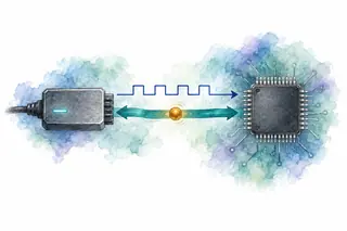
A debug probe sends SWCLK to the chip debug port. A separate bidirectional SWDIO connection carries request, acknowledgment and data, with only one driver at a time. The probe and target also share ground.
The probe supplies SWCLK, while requests and replies share SWDIO. A turnaround gives the current sender time to release that wire before the other side drives it, avoiding two outputs fighting each other.
SWCLK comes from the probe; neither side drives SWDIO during a turnaround.
Only one side drives SWDIO. Turnaround transfers ownership.
Read request · 8 clocks. The debugger selects a DP register and the read/write direction.
46 clocks across shown fields; idle cycles excluded. Field widths are schematic, not proportional to duration. Default one-clock turnaround; ORUNDETECT=0. Read cases select DP RDBUFF; the write selects DP SELECT. WAIT assumes an earlier AP access remains pending; that preceding access sequence is omitted. The target keeps ownership from OK through data and parity during a successful read. SWCLK need not run continuously while idle.
Beyond the wire transfer, ADIv5 Access Port reads are posted. Keep the requested address separate from the result returned now.
AP read A→Older value · ignoreAP read B→Value at ADP RDBUFF→Value at BRDBUFF collects the final result without starting another AP access. This separate, simplified sequence assumes the same selected AP, successful accesses, and no intervening SELECT or bank changes. Follow the target’s WAIT and error rules.
JTAG supports scan chains and boundary-scan testing. SWD provides an Arm debug connection with fewer main signal pins.
Check the chip and probe for supported ports. Neither a pin count nor a connector guarantees the target exposes the debug or test feature you need.
Ground is required. Reset, trace, and other optional signals are excluded from these counts.
Explore the JTAG chain →Advance here or in the transfer above. The highlighted operation and wire state stay on the same step.
send_request(DP_RDBUFF, READ)
release_for_turnaround()
ack = receive_ack()
if ack == WAIT:
turn_to_host(); return DEFER
word = receive_32_bits()
check_even_parity()
turn_to_host()
return wordDebug transfer in progress
Why this step mattersStep 1 of 6, Read request. The request selects a debug-port register and tells the target whether this attempt reads or writes.
These are probe-level operations, not application CPU loads. Read selects DP RDBUFF after an earlier AP access; write selects DP SELECT. The example uses one-clock turnaround, overrun detection disabled, and valid data parity. WAIT needs bounded retry or deferral. A real driver must also handle FAULT, parity errors, and sticky status using the selected debug-port specification.
Release SWDIO before the other side takes ownership.
Retry with a bound; WAIT did not return a successful data word.
This lab omits WAIT/FAULT data phases only because ORUNDETECT is disabled.
Trace the driver for every phase, verify request/data parity, then exercise OK and WAIT separately. For a memory read, also track AP selection, posted results, and error recovery.
ADIv5 wire-level examples with one-clock turnaround and ORUNDETECT disabled. Initialization, multidrop selection, power-up, and full error recovery are outside this lab; AP posting is explained but not simulated. SWCLK need not run continuously while idle.
Universal Serial Bus
Use USB when a device must connect through a computer’s host stack. Descriptors describe its functions and endpoints, and the host schedules transfers. This adds discovery and software setup, but provides a standard connection beyond a board-level byte link. These examples use USB 2.0 full-speed bulk.
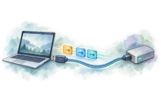
The host PHY and device PHY are connected by two continuous wires, D+ and D−, forming one differential data pair used in either direction. VBUS supplies power from the host to the device body outside the PHY. Ground connects the bodies separately and has no direction.
Each PHY converts packet bits to electrical signaling on D+ and D−, one differential data pair. Host and device take turns transmitting on that same pair; VBUS supplies power through a separate connection.
The PHY is the electrical interface; VBUS and ground connect separately from the continuous D+ / D− pair.
Time flows down. The host starts both IN and OUT transactions.
Host sends IN. The payload will travel device → host.
USB 2.0 full-speed bulk; 12 Mbit/s is raw signaling, not payload throughput. D+ and D− form one shared differential pair. The fixture begins with DATA0 expected. Packet encoding, error retries, enumeration and setup traffic are omitted. NAK does not advance the data toggle. Low-speed USB has no bulk transfers. Packet spacing is not a duration scale.
Plugging in a cable does not immediately create a data stream. Enumeration lets the host discover what the device offers.
An endpoint is a numbered data channel. Its type determines scheduling and delivery behavior; the lab follows a configured bulk endpoint.
USB addresses device endpoints and defines transactions and transfer types. UART frames bytes; an application defines how those bytes form messages.
The successful bulk handshake above is one USB case. NAK, errors, and other transfer types follow different paths.
Explore UART byte framing →Advance here or in the transfer above. The highlighted operation and wire state stay on the same step.
send_token(IN, address, endpoint)
reply = receive_packet()
if reply == NAK:
return DEFER
accept_data_and_toggle(reply)
send_ack()
return ACCEPTEDBulk transaction in progress
Why this step mattersStep 1 of 3, IN token. The host schedules IN; the token selects both the device and its endpoint.
This pseudocode expands host-controller packet handling; application firmware normally submits a USB transfer to a stack. The device is already configured, the expected PID starts at DATA0, and CRC is valid. The receiver advances its expectation when it accepts the expected DATA; the transmitter advances only after receiving ACK. NAK is temporary backpressure, not a hard failure. Bound the overall request by a deadline or cancellation policy. Real stacks also handle STALL, timeouts, retry rules, and duplicate data packets.
Both names use the host’s perspective: IN brings payload to the host.
The endpoint may be temporarily unready; the host can request again.
Other transfer types have different timing and handshake rules. Low-speed USB does not support bulk.
Check enumeration, endpoint type, token direction, payload, and handshake. Test NAK followed by a later retry, and a lost ACK without duplicate application delivery. Electrical compliance needs PHY-level measurements too.
USB 2.0 full-speed bulk after configuration. Packet fields, CRC, encoding, bit stuffing, hub timing, and electrical compliance are not simulated. USB-C describes connector/power capabilities, not the bulk transaction drawn here; USB 3.x uses additional signaling.
Ethernet · IEEE 802.3
Use Ethernet when a board needs to communicate with computers or other devices across a wired network. Unlike SPI's selected peripheral or USB's host-scheduled transfers, switched Ethernet gives each device a separate link. Start with the MAC, PHY, and one frame before adding IP addresses, sockets, or TCP.
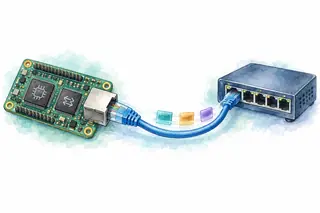
RMII is the digital connection between the MAC and PHY. The 100BASE-TX cable carries a different electrical signal.
TXD[1:0]
TX_EN→Bits + transmit enableRXD[1:0]
CRS_DV←Bits + carrier/data validMDC / MDIOPHY configuration + link statusMAC means Media Access Control: it handles frame fields and checks. The PHY, or physical-layer transceiver, turns the digital stream into cable signaling and recovers incoming data.
The clock source and PHY straps depend on the chosen parts. MDC/MDIO manages the PHY; it does not carry packet payload.
Follow one frame through ownership, transmission, and a separate peer observation. Compare local errors with corruption seen only by the receiver.
REF_CLKTXD[1:0]TX_ENNo frame from this attempt yetNo per-frame Ethernet ACK. These are separate observations; their placement does not specify a timing order between devices.
Check the negotiated link. Read the PHY's resolved speed and duplex, then configure the MAC to match before queuing a frame.
100 Mb/s, full duplex. The RMII inset shows one illustrative 0xA5 payload byte, least-significant dibit first. This is a stage model, not a cable waveform or a timing relationship between local completion and peer reception.
An untagged Ethernet II frame includes addresses and error detection. Small payloads need padding to reach the minimum frame size.
14 + 40 + 6 + 4 = 64 bytesPreamble/SFD + frame: 72 bytes → 5.76 µs at 100 Mb/sIncluding the 96-bit interframe gap: 6.72 µs per repeated minimum-frame slotThe interframe gap is idle time, not another frame field. The MAC adds padding and FCS only when configured to do so; confirm what the driver expects in memory.
Frames between network peers
Host schedules transactions
Choose Ethernet for network access, such as an instrument serving several computers through a switch. Add the required IP and transport stack for those services.
Choose USB for a host-attached device, such as a local measurement accessory. The USB class and endpoints describe how the host communicates with it.
A connector alone does not supply either software model. Both need drivers, buffering, and a defined application protocol.
Compare USB’s host-scheduled transfer →Advance here or in the transfer above. The highlighted operation and wire state stay on the same step.
if not link_up(): return LINK_DOWN
desc = try_reserve_tx()
if desc == NONE: return BUSY
fill_frame(desc, payload)
publish_to_dma(desc)
status = bounded_tx_wait()
reclaim_released(desc)
return status // local result onlyLink ready · no frame queued
Why this step mattersStep 1 of 7, Check the negotiated link. Read the PHY's resolved speed and duplex, then configure the MAC to match before queuing a frame.
Conceptual driver operations, not register-level code. publish_to_dma includes the target's cache maintenance, memory barriers, descriptor ownership change, and doorbell. bounded_tx_wait uses a configured deadline; on timeout, recovery must stop DMA access before any buffer is reclaimed. reclaim_released returns only a descriptor and buffer that DMA no longer owns. The success and bad-FCS fixtures both complete locally without a TX error. Peer reception is a separate observation for teaching, never a value returned by this TX API. The displayed stages do not define the relative timing of the two devices.
A MAC address belongs to link-layer delivery. IP addresses, routing, and transport reliability are separate mechanisms above this frame.
Local completion permits buffer reuse. It does not prove peer reception or application processing.
Publish visible data, transfer ownership, and wait for release. A timeout alone is not permission to reuse memory.
RMII joins MAC and PHY on the board. The PHY and magnetics provide the differential cable interface.
Check negotiated link mode first, then descriptor ownership, local TX status, and peer receive counters or a capture. A valid link LED does not prove frame delivery. To test corruption, inspect the receiver's FCS-error counter; ordinary packet captures may omit frames rejected by the NIC.
One 100BASE-TX full-duplex link with RMII, an untagged Ethernet II frame, hardware padding/FCS, a preconfigured destination, and no cache-coherency fault. Peer destination filtering passes and receive capacity is available. Bad FCS is injected on the link after local transmission. VLANs, gigabit PHYs, half-duplex collisions, TCP/IP setup, real DMA register layouts, and waveform-level cable encoding are outside this model.
Controller Area Network · Flexible Data Rate
Use CAN when several embedded nodes exchange control and status messages, such as a motor drive, sensor and supervisor. Each node has a controller and a transceiver. They share a bus, and the message identifier decides priority when transmission starts together. CAN FD keeps this arbitration model while allowing more data per frame.
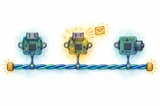
The controller builds frames. The transceiver connects its logic signals to the shared CAN_H / CAN_L pair.
Reference and power are omitted. Choose grounding or isolation to keep every transceiver within its common-mode limits. A CAN controller pin cannot connect directly to the cable.
Follow one frame, let two identifiers compete, or remove the receiver that supplies ACK.
The transmitter sends recessive; a valid receiver can overwrite it with dominant.
Queue a frame. Queuing reserves a controller transmit buffer; it does not mean the frame has reached the bus.
Logical frame phases, not an analog voltage trace. Only standard 11-bit data frames are compared; stuffed bits, CRC bits and error recovery timing are omitted.
Arbitration stays at the nominal rate. CAN FD changes the frame format and can switch to a faster data phase.
FD lengths above 8 are 12, 16, 20, 24, 32, 48 and 64. A larger buffer is not proof that a chosen DLC sends that many bytes. Check the controller’s encoding.
Several nodes publish short control messages. Define priorities, allowed senders and deadlines.
A direct byte stream suits a console or module command channel. Add message framing and responses in software.
CAN already frames and checks messages. It still needs an application contract for units, sequence numbers, stale data and command acknowledgment.
UART here means the logic-level, point-to-point link in this guide. Transceivers can adapt UART signaling to other electrical networks.
Compare UART framing →Advance here or in the transfer above. The highlighted operation and wire state stay on the same step.
frame = make_frame(0x120, [0x2A, 0x07])
queue(frame); wait_for_bus_idle()
controller.send_start_and_identifier()
controller.send_data_and_crc()
if controller.sees_ack_error():
return report_failed_attempt()
controller.check_end_of_frame()
return TX_COMPLETEQueued · not delivered
Why this step mattersStep 1 of 6, Queue a frame. Queuing reserves a controller transmit buffer; it does not mean the frame has reached the bus.
Conceptual CAN controller operations; firmware queues a frame instead of bit-banging arbitration. The fixture uses standard 11-bit data frames on a correctly terminated high-speed CAN bus. Stuffing, CRC calculation, bit timing, error counters and recovery are not simulated. The no-ACK case is one observed attempt; controller retry policy and a software deadline must be configured. Losing arbitration is normal contention, not a transmission error. An ACK does not identify its sender or prove application consumption.
Any active receiver that validates the frame can acknowledge it, even if software does not use that identifier. A command may need an explicit application response.
This high-speed linear bus uses 120 Ω at each physical end, not at each transceiver. Keep stubs short and validate the selected physical-layer design.
The lower-priority sender becomes a receiver and waits for another opportunity. Persistent higher-priority load can delay it, so budget deadlines and retries.
Check every controller, transceiver and timing configuration. Classical-only nodes may signal errors when an FD frame arrives.
Inspect identifier, payload, ACK and error status. Trigger simultaneous frames with different IDs, then remove the acknowledging receiver. Check both physical terminations, differential signaling, bit timing, retry limits and transmit completion status.
Standard 11-bit data frames on a high-speed CAN bus. Arbitration is shown without stuffed bits. The 500 kbit/s nominal and 2 Mbit/s FD data rates are fixtures, not guarantees for a cable length or transceiver. Extended IDs, remote frames, CRC calculation, detailed error confinement, bus-off recovery and higher-layer protocols are outside the simulation.
Secure Digital memory and I/O
Use SD memory to read and write stored sectors, and SDIO to control a compatible peripheral such as a wireless module. Both use host-driven clocks, but storage addresses and function registers are different things. Start with a sector read, then switch to CMD52 to see a register byte return without a DAT transfer.
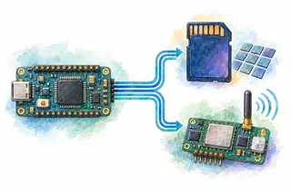
The host supplies CLK. Both sides take turns on CMD; payload uses the separate DAT bus.
The drawing shows native SD after initialization. CMD/DAT pull-ups, voltage, pin mux and routing must follow the board and device requirements. This is a signal map, not a wiring schematic.
Follow the command on CMD, then see whether the result uses DAT or returns inside the response.
CLK shows the timing source, not an elapsed-time scale. Response delays and clock gating are not drawn.
Arm a private receive buffer. Reserve 512 bytes and arm reception before requesting the block, so arriving data has somewhere to go.
Native SD · already initialized · 4-bit SDR · 12 MHz fixture. One 512-byte SDHC read or one SDIO register byte. Phase widths are not durations.
A native SD read in four-bit SDR mode carries one bit per DAT wire on each sampling edge. Two such samples assemble one byte.
512 × 8 ÷ 4 = 1,024 clocksPayload only · excludes command, response, start/end bits, CRC and waitsAt the same clock frequency, four lanes carry this payload in one quarter of the clocks. This is not a file-speed guarantee: device delays, command overhead and software still count.
Read a stored sector. A filesystem gives those bytes names, directories and file meaning.
Read a function’s status or control register. No separate DAT payload follows.
Move a byte count or blocks for an I/O function. Choose fixed-address FIFO or incrementing-address access.
A compatible connector is not enough. The host driver must support the device’s command set, initialization and function behavior.
A conventional SPI link uses one incoming data wire. Native SD uses a distinct command line and can add data lanes. Device support and available pins decide which mode is usable.
Compare SPI’s separate send and receive wires →Advance here or in the transfer above. The highlighted operation and wire state stay on the same step.
buf = reserve_private(512)
arm_read(buf, 512, timeout)
send_cmd17(block = 8) // SDHC
r1 = wait_response(timeout)
if not r1.ok: abort_release(); return ERROR
data = wait_data(timeout)
if not data.ok: discard(buf); return ERROR
return publish(buf)Block read in progress
Why this step mattersStep 1 of 6, Arm a private receive buffer. Reserve 512 bytes and arm reception before requesting the block, so arriving data has somewhere to go.
The card is already initialized, selected and in 4-bit Default Speed mode; the host matches its width and voltage. The fixture uses a 12 MHz clock, not an initialization clock. Arm the receive path before issuing CMD17. The controller handles response CRC, four data-line CRC16 checks and transfer timeouts; data.ok includes successful completion and CRC. Abort must stop hardware/DMA before releasing the private buffer. Register flags, cache maintenance, timeout values and recovery are controller-specific. A single-block read does not use a write-programming busy phase or require CMD12 to end a successful transfer.
SDHC block 8 uses command argument 8. SDSC uses byte-address units; the equivalent 512-byte sector starts at 4096.
Initialize and configure the card as well as the host. Four-bit mode requires agreement on DAT0 through DAT3.
Check command status, data completion and CRC before publishing the block. A received buffer can still contain invalid data.
SDIO function registers use CMD52/CMD53. Check the module’s register map, pin mux, pull-ups and voltage requirements.
Decode the command and its response separately from the DAT payload. Confirm width at both ends, the selected address units, the received byte count and all CRC results. Force a missing response and corrupt data before checking recovery.
Initialized and selected native-SD devices, 3.3 V, four-bit Default Speed SDR, with a fictional 12 MHz operating clock supported by both ends. The memory fixture is SDHC; the I/O fixture is an enabled SDIO function. Initialization, write programming, interrupts, UHS, DDR, SD Express and filesystems are outside the trace. Diagrams are not to scale.