
Joint Test Action Group · IEEE 1149.1
JTAG Bits move through a chain of registers
Use JTAG to inspect a chain of devices or test board connections that are difficult to probe. Shared clock and control signals move data through each device’s selected register. The instruction determines what is scanned, so chain order and register lengths are part of the setup.
JTAG wiring, timing and transaction
Wiring
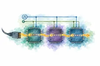
The debugger has separate TCK and TMS outputs, each connected in parallel to Device A and Device B. Curved crossings are not junctions. Data out enters A TDI, passes through A selected register and TDO, then B TDI, selected register and TDO, and returns to debugger data in.
The blue TCK and TMS branches deliver the same clock and state-control signal to both chips. The amber serial chain instead passes through each chip’s selected register before returning to the debugger.
TCK and TMS go to both chips; selected registers form the serial chain, with common ground and optional reset omitted.
JTAG scan
Capture, shift six bits through the chain, then update the output latches.
Captured A=101 and B=011. Output latches remain unchanged.
Timing and model details
Two fictional three-bit data registers; captured cells 101011; serial input 110100. Cells are drawn from TDI on the left to TDO on the right. Capture and shift leave separate output latches unchanged. Intermediate TAP states and instruction loading are omitted, so the conceptual Capture and Update buttons do not represent single-clock transitions. Not every JTAG data register drives physical pins.
Scan length follows the registers
Count the register selected inside each chip. Changing an instruction can shorten the path without rewiring the board.
BYPASS contributes one bit. These totals count shift clocks only; entering and leaving Shift-DR needs additional TAP state transitions.
JTAG or SWD for debugging?
JTAG supports scan chains and boundary-scan testing. SWD provides an Arm debug connection with fewer main signal pins.
Check the chip and probe for supported ports. Neither a pin count nor a connector guarantees the target exposes the debug or test feature you need.
Ground is required. Reset, trace, and other optional signals are excluded from these counts.
Explore SWD ownership →Follow a transaction
Advance here or in the transfer above. The highlighted operation and wire state stay on the same step.
tdo = []; capture_dr()
for bit in take(input_bits, 6):
tdo.append(shift(bit))
update_dr()
compare_latches(expected)- Who drives
- Debugger: TCK/TMS; TDO is not sampled outside Shift-DR
- Sent so far
- Capture selected registers; no bits shifted
- Response so far
- No TDO bits collected; output latches A/B = 000 / 000
Output latches unchanged
Why this step mattersStep 1 of 8, Capture. Capture loads the scan cells while the separate output latches keep their previous values.
Implementation notes
The debugger must navigate the TAP states and select the correct instruction before these conceptual operations. This model has two three-bit data registers and an independent output latch. The short-scan case deliberately updates after five clocks; JTAG does not automatically report that length mistake. The comparison is a teaching check against the intended result, not a built-in protocol ACK.
Common mistakes
Chaining the control wires
TCK and TMS reach the targets in parallel; TDI/TDO form the serial path.
Forgetting BYPASS bits
Every device placed in BYPASS still contributes one bit. Count the selected data registers, not the instruction-register lengths.
Reading newly sent bits first
The captured chain contents leave before the replacement bits reach the output.
Establish a known TAP state, confirm device order and documented register lengths, then compare the captured output with the expected serial sequence. A scan match alone does not prove a device-specific debug operation completed.
Further details and primary sources
- Select the register first
- An instruction-register scan chooses which data register each target places between TDI and TDO. The same wires can expose boundary-scan cells, identification, a one-bit BYPASS register, or a device-specific debug register.
- Capture, shift, then update
- Capture loads a snapshot. Shift clocks old bits out while new bits move in. Update applies the scanned value where that register supports an update. Intermediate TAP states connect these stages; they are not three adjacent states.
- Count every selected register
- The scan length is the sum of all selected register lengths. BYPASS leaves a one-bit path through an otherwise uninteresting target; it does not remove that device electrically. Boundary Scan Description Language (BSDL) files document the relevant device structure.
Example scope
A selected data-register scan, not a complete TAP or processor debugger. The lab’s registers have explicit capture and update storage. Actual instructions define whether an update changes pins, internal state, or nothing.
Primary sources
Updated