
Secure Digital memory and I/O
SD / SDIO Storage blocks or peripheral registers
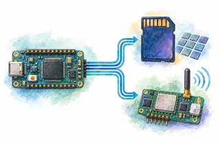
Use SD memory to read and write stored sectors, and SDIO to control a compatible peripheral such as a wireless module. Both use host-driven clocks, but storage addresses and function registers are different things. Start with a sector read, then switch to CMD52 to see a register byte return without a DAT transfer.
SD / SDIO wiring, timing and transaction
One command line, four data lines
The host supplies CLK. Both sides take turns on CMD; payload uses the separate DAT bus.
The drawing shows native SD after initialization. CMD/DAT pull-ups, voltage, pin mux and routing must follow the board and device requirements. This is a signal map, not a wiring schematic.
A sector read and a register read
Follow the command on CMD, then see whether the result uses DAT or returns inside the response.
- 1Prepare
- 2CMD17
- 3R1
- 4Payload
- 5CRC
- 6Finish
- CMD
- Released
- DAT3…0
- Released
CLK shows the timing source, not an elapsed-time scale. Response delays and clock gating are not drawn.
Arm a private receive buffer. Reserve 512 bytes and arm reception before requesting the block, so arriving data has somewhere to go.
Timing and model details
Native SD · already initialized · 4-bit SDR · 12 MHz fixture. One 512-byte SDHC read or one SDIO register byte. Phase widths are not durations.
Four bits per payload clock
A native SD read in four-bit SDR mode carries one bit per DAT wire on each sampling edge. Two such samples assemble one byte.
512 × 8 ÷ 4 = 1,024 clocksPayload only · excludes command, response, start/end bits, CRC and waitsAt the same clock frequency, four lanes carry this payload in one quarter of the clocks. This is not a file-speed guarantee: device delays, command overhead and software still count.
Storage sectors or I/O registers?
Read a stored sector. A filesystem gives those bytes names, directories and file meaning.
Read a function’s status or control register. No separate DAT payload follows.
Move a byte count or blocks for an I/O function. Choose fixed-address FIFO or incrementing-address access.
A compatible connector is not enough. The host driver must support the device’s command set, initialization and function behavior.
A conventional SPI link uses one incoming data wire. Native SD uses a distinct command line and can add data lanes. Device support and available pins decide which mode is usable.
Compare SPI’s separate send and receive wires →Follow a transaction
Advance here or in the transfer above. The highlighted operation and wire state stay on the same step.
buf = reserve_private(512)
arm_read(buf, 512, timeout)
send_cmd17(block = 8) // SDHC
r1 = wait_response(timeout)
if not r1.ok: abort_release(); return ERROR
data = wait_data(timeout)
if not data.ok: discard(buf); return ERROR
return publish(buf)- Who drives
- Host supplies CLK; CMD and DAT released
- Sent so far
- No command sent
- Response so far
- No response yet
Block read in progress
Why this step mattersStep 1 of 6, Arm a private receive buffer. Reserve 512 bytes and arm reception before requesting the block, so arriving data has somewhere to go.
Implementation notes
The card is already initialized, selected and in 4-bit Default Speed mode; the host matches its width and voltage. The fixture uses a 12 MHz clock, not an initialization clock. Arm the receive path before issuing CMD17. The controller handles response CRC, four data-line CRC16 checks and transfer timeouts; data.ok includes successful completion and CRC. Abort must stop hardware/DMA before releasing the private buffer. Register flags, cache maintenance, timeout values and recovery are controller-specific. A single-block read does not use a write-programming busy phase or require CMD12 to end a successful transfer.
Common mistakes
Mixing block and byte addresses
SDHC block 8 uses command argument 8. SDSC uses byte-address units; the equivalent 512-byte sector starts at 4096.
Widening only one end
Initialize and configure the card as well as the host. Four-bit mode requires agreement on DAT0 through DAT3.
Trusting DMA completion alone
Check command status, data completion and CRC before publishing the block. A received buffer can still contain invalid data.
Treating every SD device as storage
SDIO function registers use CMD52/CMD53. Check the module’s register map, pin mux, pull-ups and voltage requirements.
Decode the command and its response separately from the DAT payload. Confirm width at both ends, the selected address units, the received byte count and all CRC results. Force a missing response and corrupt data before checking recovery.
Further details and primary sources
- Initialize before widening the bus
- Discover the device and its capabilities, select it, and configure both ends for the same width and timing mode. This lab starts after initialization; switching only the host to four bits does not configure the card.
- Separate responses from data
- CMD17 returns R1 on CMD, then the block on DAT. Native SD read data includes CRC16 on each active data line. DAT0 busy signaling is relevant to operations such as write programming; it is not an extra phase of the read shown here.
- Choose memory or I/O commands
- CMD17 reads a memory block. SDIO CMD52 accesses one function-register byte in its R5 response. CMD53 carries a byte count or blocks on DAT, with fixed-address FIFO or incrementing-address access as required by the function.
Example scope
Initialized and selected native-SD devices, 3.3 V, four-bit Default Speed SDR, with a fictional 12 MHz operating clock supported by both ends. The memory fixture is SDHC; the I/O fixture is an enabled SDIO function. Initialization, write programming, interrupts, UHS, DDR, SD Express and filesystems are outside the trace. Diagrams are not to scale.
Primary sources
Updated